1. Synthesis and Applications of New Nanomaterials using Electron / Ion Beam Irradiation
1) Synthesis of New Nanomaterials using Beam Irradiation
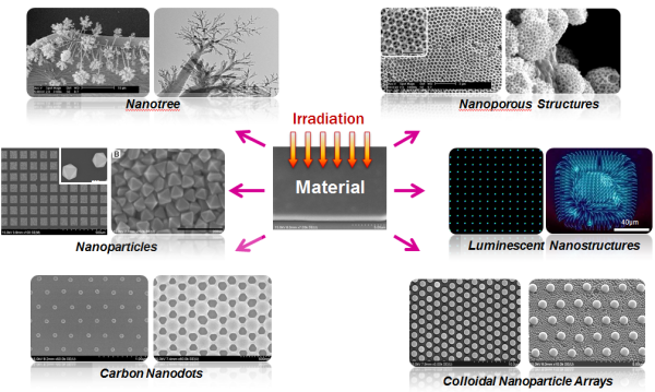
When a charged beam such as electron / ion beam is irradiated on a material, a chemical structure of the material can be completely changed, so it is possible to synthesize a new material which is completely different from the original material or to change physical / chemical / mechanical / electrical / optical properties of the original material entirely. Besides, the size of electron and ion which consist electron / ion beam is femtometer(10-15m) scale, so it is a good tool for synthesizing materials with nanometer(10-9m) scale. Especially, electron / ion beam have charges, so when electric field of the charged beams is changed, shapes or characteristics of nanostructures can be modified as you want. As it is shown in the left image, the technique for synthesizing new / nanomaterials using electron / ion beam can produce new / nanomaterials with various structures and characteristics in large quantities using just one simple procedure: beam irradiation. To synthesize new / nanomaterials using beam irradiation is our research group’s unique technique, and to operate beam irradiation is so easy that even high school students can follow, but beam irradiation is a high technology that requires brilliant ideas and research experiences.
2) Applications of Nanomaterials
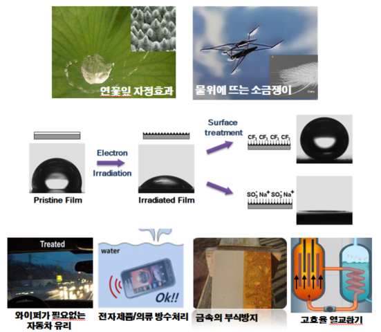
A water drop cannot attach on a leaf of lotus, and a water strider can walk on the surface of water. The reason why these phenomena happen is because the surface of a lotus leaf and a water strider has a unique micro / nano-hierarchical structure. Our research group found when a specific material is irradiated with an electron beam, the material can have a special hierarchical structure as it is shown in the left image. Using this knowledge, we developed a technique to make surfaces have superhydrophobic properties that a single water drop cannot be stained on the surface and superhydrophilic properties that water can be soaked through the surface very easily. By this technique, we are currently developing a coating technique that prevents corrosion of metal due to humid, a process to make electronic devices and clothes waterproof, a coating technique that prevents frost or dew on glasses and mirrors and a technique that improves heat transference properties of a heat exchanger.
Also, metal nanoparticles have special physical and chemical properties so that they can have important roles in a field of nanotechnology and biotechnology. Especially, precious metal nanoparticles such as gold and silver nanoparticles can be used in optics, sensing biochemical materials, catalysis and surface enhanced Raman scattering (SERS) due to their plasmonic properties depending on their size, so many researchers are working on this field.
Among above several applications, SERS is a powerful method to detect a tiny amount of biochemical and radioactive materials on the surface of precious metals. Intensity of Raman scattering of biochemical and radioactive materials is maximized on the surface of nanostructured metal. This increase of Raman scattering is possible because of an increased electromagnetic field due to localized surface plasmon resonance (LSPR).
Using this mechanism, we are currently developing a technique to detect a tiny amount of harmful biochemical and radioactive materials or to trace high value materials such as rare earth resources on real time.
2. Synthesis and Applications of New Materials for Energy and Environmental use using Beam Irradiation
1) Synthesis of Optical Semiconductors using Beam Irradiation and Decomposition of Environmental Contaminants using the Optical Semiconductors
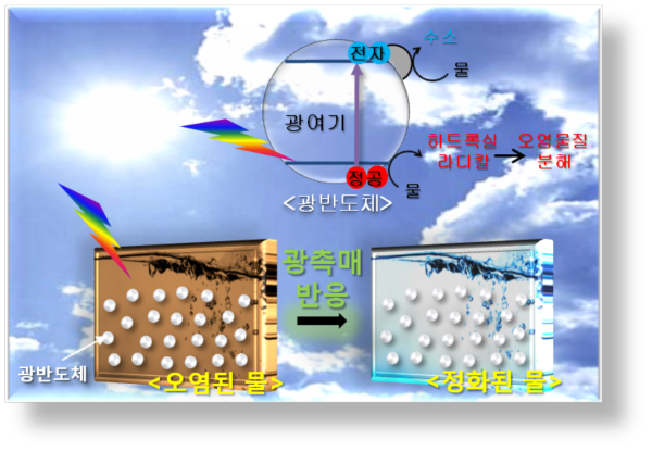
Decomposition of environmental contaminants using optical semiconductors has been highlighted. This technology is a very simple process that nanoparticles dispersed in polluted water with sunlight destroy aquatic environmental contaminants, and have advantage that it requires any expensive equipment or does not leave byproducts. A key point of this technology is how much sunlight is absorbed by optical semiconductors, and how well electrons and holes produced by absorbed sunlight react with water at the surface of the optical semiconductors. Since these things related to the size of band gap of optical semiconductors and the location of valence bands and conduction bands(in case of organic materials, LUMO and HOMO), a technology to control valence bands and conduction bands is very important. In this context, performance of the optical semiconductors can be improved by characteristics of electron beam irradiation which can control molecular structures of conventional materials, the size of band gap of irradiated materials controlled by differentiating electron beam dose and the position of valence bands and conduction bands.
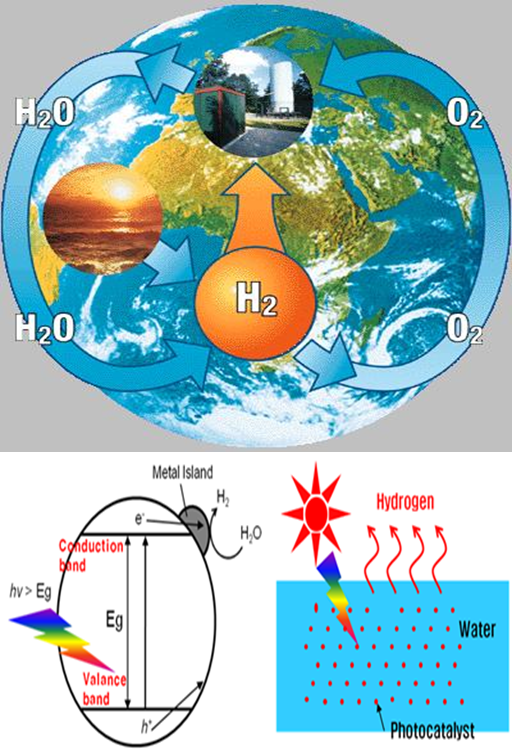
2) Fabrication of Photocatalyst and Photocatalytic Water Splitting for Hydrogen Production
Photocatalytic hydrogen production is clean hydrogen production technology. Hydrogen can be achieved by water splitting, and becomes water after combustion. However, conventional hydrogen production technology is dependent on fossil fuel and electricity. Therefore, the unconventional technology for hydrogen production that maximize the merits of hydrogen should be developed. Photocatalytic water splitting produces hydrogen from water using sun light which is clean and sustainable.
While semiconductor materials absorbs sun light with higher energy than its band gap energy, the semiconductor produces electron-hole pairs. the electrons on conduction band reduces water and produces hydrogen. Through the simple process illuminating sun light into semiconductor powders dispersed in water, hydrogen can be produced without residual pollutant.
This research has two main tasks. At first, the photo-generated electron-hole pairs should be separated and transferred to surface of particles to suppress charge recombination. For this purpose, noble metal deposition, addition of electron donor has been studied. Our group is trying to simplify the process for noble metal loading and enhance the charge transfer by electron beam irradiation. The other main task is utilization of visible light. The photon has energy which is inversely proportional to its wave length. Therefore, semiconductor materials with high band gap energy only absorbs UV light with wave length shorter than 400 nm. However, most of the sun light is composed with visible light. For fabrication of photocatalyst with high conversion efficiency, utilization of visible light is essential. Our group is trying to narrow band gap using bad gap tuning technology by electron irradiation for visible light-driven photocatalytic water splitting.
3. Development of Organic Semiconductors and Organic Electronic Devices using Electron Beam Irradiation
As we refer 21st century as the era of the semiconductor, the semiconductors are used in our lives in almost anywhere with the recent huge development of electronic engineering. However, the harmful fabrication processes and the high price of existing silicone-based semiconductor become the constraints for new applications such as "wearable-computer".
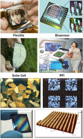
As an alternative to this, organic semiconductor based on a organic (carbon) has been emerged because of its many advantages; easy and environmental manufacturing processes, economical raw materials, suitable for biological applications. Therefore, the various research groups present researches about the production of material and the associated devices like organic solar cells with high efficiency, flexible organic displays and so on.
However, the conventional methods of manufacturing an organic semiconductors are hard to control its properties directly and the fine pattern, which is essential to sophisticated devices, is hard to be achieved. Therefore, by using an unconventional electron beam irradiation, we are doing the research about improving or newly creating of the semiconductor material, and producing a fine pattern of nano or micro scale.
In particular, despite the short research period, our laboratory show world-class technique and performance in organic transistor field and various multi-faceted researches are progressed for the goal of commercially available real applications.
4. Advanced X-ray Tube for Medical and Industrial Applications / Small Accelerator
1) Advanced X-ray Tube for Diagnosis and Therapy of Cancer
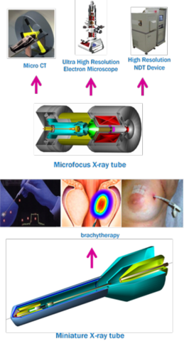
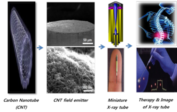
An X-ray tube is a vacuum tube that produce X-ray when accelerated electrons collide with X-ray target material. All of commercial X-ray tube adopt a thermionic emission type using tungsten filament as electron source. The thermionic type is emission of electrons from a filament in the vacuum. The thermionic type has a disadvantage of increasing temperature of entire X-ray tube during operating. So it has limitation to decrease X-ray tube size. On the other hand, Field emission type that is emission of electron induced by applying high voltage sharp tip such as carbon nanotube can improve this heating problem. X-ray tube are widely used for medical and industrials field. The X-ray focal spot size reduce to get high resolution X-ray image. Our research group has an original technology of micro-focus X-ray tube fabrication. As well as miniature X-ray tube under development take center stage of cancer therapy as replacement of isotope. The miniature X-ray tube can minimized optimized the patient's pain, shorter duration time of cancer treatment and minimized damage to normal cell. And miniature X-ray tube can reduce x-ray exposure of human body. The development of miniature X-ray tube is advanced medical research field to improve cancer therapy innovatively.
2) Development of Highly Stable Carbon Nanotube Field Emitters for Miniature X-ray Tubes
For conventional radiation sources, generally radioisotopes such as Ir-192 were used for brachytherapy. The radioisotopes can be used at the narrow space through a metal wire tube due to the small size of radioisotopes. However, the radiation was always emitted from radioisotopes, and thus, external shielding materials are necessarily. Therefore, when the radioisotopes were used for brachytherapy, the risk for radiation exposure and the operation price are relatively high.
However, if miniature X-ray tubes were used for brachytherapy, the radiation emission from X-ray tubes can easily control by switching on/off buttons. Such miniature X-ray tubes are also separated into 2 parts by the production method of the free electron from cathode. Conventional thermionic-type X-ray tube has some advantages semi-permanent life time, controllable tube voltage, current and on/off. However, the main drawback of this method is high temperature of filament (cathode) to produce the free electrons. The operation temperature of the thermionic cathode should be normally higher than 1500°C. So, the reduced size of X-ray tube has been limited by the use of cooling device, which increases the size of the miniature X-ray tube. To further decrease the size of miniature X-ray tube, recently field emission-type miniature X-ray tube is focused due to cold emission process. It does not increase the temperature of X-ray tube because free electrons are generated just by high electric field. So, the X-ray tube does not need the cooling device. In this sense, it is expected that more miniaturized X-ray tube down to several millimeter could be realized. Such the use of miniature X-ray tube could reduce the pain of patient during cancer treatment.
However, for miniature X-ray tube, arcing events (vacuum breakdown or sparking) is an inevitable factor in the field emission at high electric field and arcing event is an irreversible catastrophic phenomenon for a device operation. So for the future performance of the X-ray tubes, highly stable field emitters against arcing should be developed and arcing events have to be prevented. For this goal, our laboratory is experimenting about development of highly stable field emitters against arcing event.